
Knowde Enhanced TDS
Identification & Functionality
- Product Type
- Technologies
- Product Families
Features & Benefits
- Labeling Claims
- Ready-to-Use Product Features
- Attributes
- Low melting lead-free solder paste based on tin/bismuth alloys.
- Clear, pin-testable flux residue.
- Halide and halogen free. No intentionally added halogens (Zero halogens).
Applications & Uses
- Applications
- Application Area
- Cleaning
Raw solder paste can be removed from the stencil, squeegee blades, and circuit boards using a variety of commercial cleaners. Isopropyl alcohol (IPA) can also be used.
After reflow, no-clean solder paste residues are designed to be “safe” and do not need to be removed from the circuit board. If removal of the flux residues is desired, then a commercial cleaning agent should be used. Several common cleaning agents have been tested and found to be effective.
Properties
- Physical Form
Technical Details & Test Data
- NC722 with Solder Alloy
Solder Alloy Solder Powder Size Availability
(IPC J-STD-005)Melting Range (°C) Sn42/Bi58 Type 3 138°C Sn42/Bi57/Ag1 Type 3 138 - 140°C - Other sizes of solder powder are available upon request.
- The size range for the solder powder types are as follows:
- Type 3 (25-45 μm >80%). Mesh -325/+500
- Type 4 (20-38 μm >80%). Mesh -400/+635
- Type 5 (15-25 μm >80%). Mesh -500/+800
- Compatible Products
- NC120, NC160, NC165 liquid fluxes.
- NC26 gel flux.
- Technical Details
Print Parameter Preferred Acceptable Solder paste bead size 1.5 to 2.0 cm (0.60 to 0.80 in) 1.0 to 2.5 cm (0.40 to 1.0 in) Squeegee blade Fine grain stainless steel. 60° from horizontal. 45° from
horizontal for pin in paste.Any type of stainless steel Stencils Fine grain (2-5 µm) or ultra-fine
grain (1-2 µm) stainless steelAll types of commercially
available stencilsPrint speed 30 to 100 mm/sec (1.2 to 4.0 in/sec) 20 to 200 mm/sec (0.8 to 8.0
in/sec)Pressure / blade length
(increase with increasing speed)0.18 to 0.27 kg/cm (1.0 to 1.5 lbs/in) 0.18 to 0.54 kg/cm (1.0 to 3.0
lbs/in)Separation speed 1.0 to 5.0 mm/sec 0.5 to 10.0 mm/sec Underside stencil cleaning Wet / vacuum / vacuum cycle every 1-5 prints Other cleaning cycles every 1 to 20 prints depending upon
technologyStencil life 4 hours at 18-29°C (65-85°F) and 10-70% RH. Stencil life may be shorter outside of the preferred
conditions.- Blade pressure should be set as low as possible to clean off the stencil. Higher blade pressures will increase stencil and blade wear, and can lead to “scooping” and other print defects.
- Underside stencil cleaning is best accomplished with commercial cleaners and high quality wipe materials. Nano-coated stencils can be used to reduce the frequency of underside cleaning.
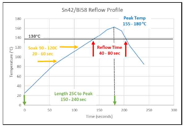
Reflow Parameter Preferred Acceptable Profile length
(25°C to peak)2.5 to 3.5 min (150 to 210 sec) 2.5 to 4.0 min (150 to 240 sec) Heating ramp rate
(20 second window)1.0 to 2.0°C/sec 1.0 to 3.0°C/sec Preheat / soak time
(90 - 120°C)20 to 40 sec 20 to 60 sec Peak temperature 155 to 175°C 155 to 180°C Reflow time
(time above liquidus)50 to 70 sec 40 to 80 sec Cooling ramp rate
(20 second window)3.0 to 6.0°C/sec 1.0 to 6.0°C/sec - Reflow time should be calculated based on the liquidus point of the alloy used: Sn42/Bi58 = 138°C, Sn42/Bi57/Ag1 = 140°C.
An example reflow profile graph is shown below. This is a good starting point but it can be modified to fit the product and process. Contact FCT Assembly for assistance with reflow profiling.
 Sn/Bi alloys should not be mixed with lead (Pb) bearing metals. If Pb is mixed with Sn and Bi, then a very low melting (approx. 95 °C) intermetallic compound can form. This very low melting Sn/Bi/Pb compound may cause solder joint failure due to heating during operation of the electronics.
Safety & Health
- Safety
Wear chemically resistant gloves when handling solder paste. Avoid breathing fumes, especially during reflow of the solder paste.
J-STD-004B Flux Standard Test Method Result J-STD-004B classification J-STD-004B methods ROL0 Halide ion content (Br- , Cl- , F- , I- ) IPC 2.3.28.1 0.0 % wt Halogen content (Br and Cl) EN 14582, IPC 2.3.28.1 0.0 % wt Halide by silver chromate IPC 2.3.33 No halides detected Fluoride by spot test IPC 2.3.35.1 None detected Copper mirror IPC 2.3.32 Low activity Copper corrosion IPC 2.6.15 No corrosion Surface Insulation Resistance (SIR) IPC 2.6.3.7 Pass Electro Chemical Migration (ECM) IPC 2.6.14.1 Pass J-STD-005 Solder Paste Standard Test Method Result Viscosity - Brookfield IPC 2.4.34 Refer to the C of A Slump - frosted glass IPC 2.4.35 Pass Solder balling - frosted glass IPC 2.4.43 Acceptable Wetting - copper IPC 2.4.45 Pass Tack force IPC 2.4.44 30 gram force typical
Packaging & Availability
- Packaging Type
- Solder Paste Packaging
Solder Paste Packaging Net Weight (grams) Jars 250, 500 Cartridges 500 or 600 (6 oz), 700 (8 oz), 1300 (12 oz) Syringes 30, 100 Enclosed print systems 800
Storage & Handling
- Storage and Handling
Best practices for storage and handling of solder paste are listed below.
- Shelf life is 6 months when stored at 0 to 10°C (32 to 50°F).
- Warm the solder paste to room temperature (18 to 29°C / 65 to 85°F) before use. Do not force warming by heating the solder paste. Keep the solder paste sealed while warming, which typically takes 3 to 4 hours at room temperature. Warming overnight is acceptable.
- Ideally solder paste should be mixed before use to bring it to a normal working consistency. This can be done by hand-stirring in a jar, or using a knead cycle on the printer.
- Best practice is to keep the solder paste at room temperature until completely used. Remaining fresh solder paste should be sealed in the original container along with all inserts, lids, etc.
- If solder paste is removed from the printer and stored, it is recommended to store it in a separate container from the fresh solder paste. The container should be sealed with all inserts, lids, etc.
- Once solder paste is applied to the circuit board, the best practice is to reflow the solder paste as soon as possible. It is acceptable to reflow within approximately 4 hours.